
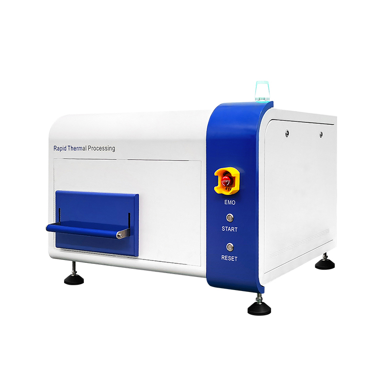
The rapid annealing furnace uses halogen infrared lamp as the heat source to heat the material to the required temperature through rapid heating, so as to improve the crystal structure and optoelectronic properties of the material.
Its features include high efficiency, energy saving, high degree of automation and uniform heating.
In addition, the rapid annealing furnace also has high temperature control accuracy and temperature uniformity, which can meet the needs of various complex processes.
The rapid annealing furnace adopts advanced microcomputer control system, combined with PID closed-loop temperature control technology, to ensure high temperature control accuracy and temperature uniformity.
The extremely fast heating rate is achieved through efficient heat sources such as halogen infrared lamps, and the wafer is quickly heated to a predetermined temperature, so as to eliminate some defects in the wafer and improve its crystal structure and optoelectronic properties.
This high-precision temperature control is very important to the quality of the wafer and can effectively improve the performance and reliability of the wafer.
In the process of wafer fabrication, the application of rapid annealing furnace includes but is not limited to the following aspects:
1. Optimization of crystal structure: high temperature contributes to the rearrangement of crystal structure, eliminates lattice defects and improves the order of crystals, thus improving the electronic conductivity of semiconductor materials.
2. impurity removal: high temperature RTP rapid annealing can promote the diffusion of impurities from semiconductor crystals and reduce the concentration of impurities.
This helps to improve the electronic properties of semiconductor devices and reduce the energy levels or electron scattering caused by impurities.
3.Substrate removal: in the CMOS process, rapid annealing furnaces can be used to remove substrate materials, such as silicon oxide or silicon nitride, to form ultra-thin SOI (insulator on silicon) devices.

With the rapid development of the semiconductor industry, the market demand of rapid annealing furnace continues to grow.
Rapid annealing furnaces are more widely used, especially in the fields of thin film transistors, integrated circuits, silicon-based and third-generation semiconductors.
Generally speaking, the rapid annealing furnace is the key equipment in the semiconductor manufacturing process, which has the characteristics of high precision, high efficiency and high flexibility, which is of great significance to improve the wafer performance and promote the development of the semiconductor industry.


 Home
Home