In the field of power electronics, IGBT (Insulated Gate Bipolar Transistors) is an important power device, and its packaging technology directly affects the performance and reliability of the device. This article will introduce you to the key role of DBC substrates in IGBT packaging, and how vacuum plasma activation technology can improve the performance of DBC substrates, thereby improving the reliability of IGBT packaging.
一、What is a DBC substrate?
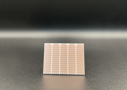
DBC (Direct Bond Copper Ceramic Substrate) is a composite material that directly bonds copper foil to the surface of an alumina or aluminum nitride ceramic substrate. It is mainly used as a chip carrier in power electronic modules. The DBC substrate completes the connection of part of the chip's connection electrodes or connection surfaces through a surface copper layer, and its function is similar to that of a PCB board. It has the characteristics of good insulation performance, good heat dissipation performance, low thermal resistance coefficient, matching expansion coefficient, excellent mechanical properties, and good welding performance.

*Tuyuan Network, intrusion and deletion
The preparation process of DBC substrates includes the following steps: first, surface treatment of copper and ceramics, and then stacking them and placing them in a vacuum high-temperature furnace for soldering. Next, the copper on the ceramic surface is chemically etched to produce designed patterns and lines. Finally, the ceramic substrate is cut with a laser and singulated to obtain a single core. DBC substrate is made of eutectic sintering of a ceramic substrate and copper foil at high temperatures. It has good electrical and thermal conductivity and high reliability, and is widely used in IGBT, LD and CPV packaging and other fields.
二、Vacuum plasma activation technology improves DBC substrate performance
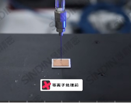
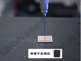
In order to further improve the performance of DBC substrates in IGBT packages, vacuum plasma activation technology is used to improve the bonding quality and improve the reliability of IBGT packages. The following are the main advantages of this technology:1. Improve bonding quality Vacuum plasma activation technology can form a uniform active layer on the surface of the DBC substrate, improve the bonding strength between the copper foil and the ceramic substrate, reduce the interface resistance, thereby improving the thermal conductivity and electrical properties of the DBC substrate. 2. Optimize microstructure Vacuum plasma activation technology can optimize the microstructure of DBC substrates, make them denser, and improve mechanical strength and thermal shock resistance. 3. Improve package reliability The DBC substrate processed with vacuum plasma activation technology has higher reliability during the IGBT packaging process, which helps to reduce failure rates and improve the overall performance of the device.

