
Microwave PLASMA
Microwave plasma assisted semiconductor packaging process

With the continuous development of technology, the requirements for semiconductor packaging are becoming higher and higher, and microwave plasma cleaning, as a means of improving packaging quality, has become an indispensable process. The purpose of cleaning is to thoroughly remove particles, organic and inorganic impurities from the surface of the equipment to ensure product quality. At present, plasma cleaning technology has been highly valued and widely recognized by society due to its outstanding advantages.
1、 Chip bonding pre-treatment
Remove surface pollutants from materials, remove oxides, facilitate solder reflow, improve chip carrier connection, reduce delamination, and improve thermal dissipation performance.
2、 Metal bonding pre-treatment
Remove organic pollutants from metal solder pads, remove thin contaminated surfaces, and improve bonding strength and uniformity of bonding wire tension.
3、 Photoresist removal
Remove residual photoresist and other organic compounds, activate and roughen the wafer surface, and improve the wetting performance of the wafer surface.
4、 Plastic sealing pre-treatment
Remove surface pollutants from the material, firmly bond the chip surface with the plastic packaging material, and reduce the generation of defects such as delamination and bubbles.
Semiconductor packaging
PLASMA processing overall solution
A microwave processing integrated solution designed for semiconductor packaging needs, which can provide microwave plasma automation systems based on product characteristics and customer needs, and offer a comprehensive online and cavity product series for selection.

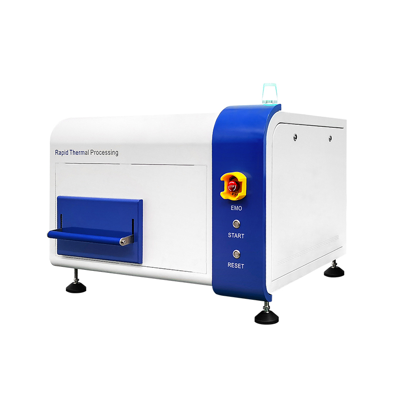
SPV-100MWR is a microwave plasma cleaning machine used in semiconductor packaging processes, equipped with a magnetic fluid rotating frame to increase plasma processing uniformity, efficient and uniform microwave plasma output, and ensure etching efficiency.

SPV-24M is an ideal choice for achieving cleaning, activation, debonding, and etching effects in semiconductor chip bonding pre-treatment, plastic packaging pre-treatment, photoresist removal, etc.

SPE-302E is a plasma debonding machine designed specifically for 8-12 inch wafers. Based on the principle of remote plasma (RPS) source etching, achieve automated peeling of photoresist for large-sized crystal circles.

SPE-152E is a plasma debonding machine designed specifically for 4-6 inch wafers. Based on the principle of remote plasma (RPS) source etching, achieve automatic peeling of small-sized crystal photoresist.


 Home
Home