
How to improve the reliability of microelectronic packaging?
With the continuous advancement of technology, the precision requirements for semiconductor IC processes and packaging processes have also increased. The residual photoresist in the semiconductor chip manufacturing process can significantly affect the related process quality of the chip during production, thereby reducing the reliability and product qualification rate of the chip. Radio frequency plasma technology cannot meet the demand for high-precision debonding and can easily lead to chip damage. By using Shengding's domestically pioneered microwave plasma technology, combined with RF bias technology, residue on the chip surface can be completely removed, significantly improving manufacturability, reliability, and yield.

IC manufacturing process flowchart

Chip packaging and testing process flowchart
What is microwave plasma?
When sufficient energy is applied to a gas, it will ionize into a plasma, such as electrons, atoms, atomic groups, free radical groups, etc. There are three common excitation frequencies for plasma power supplies: ultrasonic plasma power supplies with an excitation frequency of 40kHz, radio frequency plasma power supplies with an excitation frequency of 13.56MHz, and microwave plasma power supplies with an excitation frequency of 2.45GHz. Microwave plasma is a gas that is excited by high-energy microwave, making it a microwave plasma.
The application of microwave plasma in electronic packaging
(1) FC packaging microwave plasma treatment: Flip soldering (FC) refers to the connection of the active side of an integrated circuit chip facing downwards to the carrier or substrate. The interconnection between chips and substrates is achieved through the convex structure on the chip and the bonding material on the substrate. This can achieve both mechanical interconnection and electrical interconnection simultaneously. At the same time, in order to improve the reliability of interconnection, bottom fillers are added between the chip and the substrate. For high-density chips, flip chip soldering has strong advantages in both cost and performance, and is the development trend of chip electrical interconnection.
In flip chip packaging, after the solder balls of the flip chip are docked with the substrate solder pad, and after cleaning the flux, plasma cleaning is still required between the chip and substrate to remove surface organic contamination and reactivate the surface. This greatly improves the fluidity of the adhesive during underfill, allowing it to completely cover the flip chip and substrate without causing voids, reducing filler loss, and improving sealing strength, Reduce the generation of holes during heating, improve product reliability and lifespan.

(2) Wafer Plasma Residual Removal: In the silver paste bonding chip process, resin diffusion causes contamination or organic solvents volatilize during the curing process, and some volatile substances will deposit on the circuit surface, causing trace contamination on the chip, bonding or solder ring surface. To remove the contamination of organic solvents, microwave plasma cleaning is required before wire bonding after solidification of the chip.

(3) Metal bonding pre-treatment: The quality of wire bonding has a decisive impact on the reliability of microelectronic devices. The bonding area must not contain any pollutants. Microwave plasma cleaning can eliminate small dirt on the surface of the gold plating layer, effectively improve the wettability of the welding surface, enhance the mutual fusion of welding materials, and thus effectively enhance the strength of lead welding.

(4) Wafer surface activation: Microwave plasma cleaning can improve the hydrophilicity and increase wetting performance of the substrate material surface, provide a good contact surface, and improve the fluidity of eutectic solder and epoxy resin materials on the surface. It can effectively prevent or reduce the generation of welding voids, ensuring high reliability of adhesion and thermal conductivity.

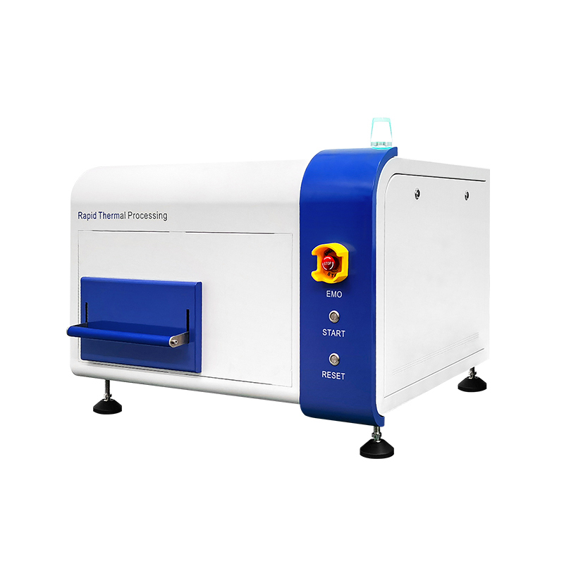
Advantages of Microwave Plasma Cleaning Machine in Packaging
The process gas is excited by a high-energy microwave electromagnetic field to ionize and generate plasma, which directly acts on the surface of the product for cleaning, activation, debonding, and etching.

Application Cases in the Semiconductor Industry
① Lead frame processing:

② Fr4 board etching:


 Home
Home