Wafer manufacturing is a high-precision and high-tech manufacturing process, and each step requires strict control of conditions to ensure that the quality of chips meets the requirements.
However, there is a detail that is easily overlooked in wafer manufacturing, which is the wettability of the wafer surface. In the production and manufacturing process of semiconductor wafer materials, surface wettability is crucial. For example, when microelectronic devices on a wafer need to be deposited or coated, poor surface wettability can lead to uneven coating thickness or film defects.

*Image source: Tom talks about smart chip manufacturing
In addition to the deposition and coating issues mentioned above, the wettability of the wafer surface can also have a certain impact on the wafer during cleaning. A hydrophilic surface can allow the wafer to come into better contact with the cleaning solution, achieving a more ideal and effective cleaning effect; On the contrary, contact between hydrophobic surfaces and cleaning solution will form water droplets, resulting in poor cleaning effect and adverse effects on subsequent processes, leading to losses. Therefore, measuring the surface contact angle has become an indispensable step in the wafer manufacturing process.

Outstanding advantages of Shengding contact angle measuring instrument
Shengding Precision has been focusing on the research and development of contact angle measuring instruments for more than ten years, committed to providing professional surface detection solutions for global users. I am a participant in the formulation of the National Contact Angle Standard (GB/T 30693-2014).
Compared with the contact angle analysis functions of domestic and imported products on the market, the Shengding contact angle measuring instrument has eight major analysis functions, including "online contact angle analysis" and "spread size analysis".

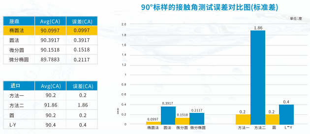
At the same time, the Shengding contact angle measuring instrument uses high-precision fitting methods to obtain more accurate detection results and smaller measurement error values.

*From the data in the above figure, it can be seen that the error values of all items in the Shengding contact angle test are lower than those of the imported contact angle measuring instrument
Fully automatic wafer type SDC-500W
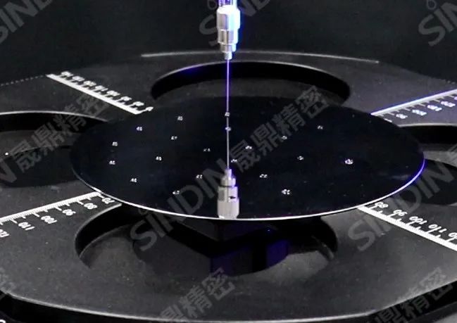
The SDC-500W contact angle measuring instrument is used for the detection of wafer surfaces. By measuring the size of the contact angle formed by liquid droplets on the wafer surface, the hydrophilicity and hydrophobicity of the wafer surface are analyzed. Can simultaneously meet the multi-point testing of 6-12 inch wafer samples.

Product advantages
① Multi point matrix testing
Matrix type multi-point testing, precise and convenient testing. Compared to existing measuring instruments from other brands that can measure up to 12 points, the Shengding wafer model can measure up to 50 points at once, and can directly display and save data in the original image, exporting the data spectrum with one click.

② Sample stageunique design
Specially designed for wafers, easy to access and measure.


